
In the autumn of 2010, a video of a sixteen-bit ALU in Minecraft by theinternetftw went viral. A month later, I’d bought the game, played around with circuits a bit and published a detailed description of a functionally identical (but much smaller) ALU on the Minecraft forum – although not exactly in that order.
Due to changes in the Minecraft forum you can now only read the original thread if you’re logged in, and the formatting is messed up, so I’m reposting it here.
By functionally identical, I mean that my ALU has the same instruction set as theinternetftw’s – the Hack instruction set developed for the book The Elements of Computing Systems. I haven’t read the book, but there’s enough information available online to implement the ALU and most other components.
I didn’t copy any part of theinternetftw’s implementation, but I did use pre-existing XNOR gates and adders as noted in the text.
Minecraft is a moving target, but the ALU still works perfectly (and performs much better). If I built it today, I’d consider using repeaters for the data and control busses, but probably stick with torches because repeaters still aren’t implemented in Redstone Simulator. (Repeaters are simpler, and also give you a signal speed of 18 blocks per cycle if you use them well. Torches can do 17, but only 16 in tightly packed parallel busses.)
Some references:
- The preface to the book
- Slides on the Hack architecture (which I found after the initial implementation, but they helped clear some things up).
Original posts follow. They’re largely unedited, so they reflect the evolution of the ALU.
Imitating Greateness: 16-bit Hack ALU Design
29 October 2010 – 16:06 (UTC+1)
Like one or two other people, I saw theinternetftw’s ALU video (and the sequel). I also wondered how it worked, or rather, how one might go around designing such a thing.
A few days later I bought Minecraft and started playing.
Today, I implemented what I believe is a functionally identical ALU in MCRedstoneSim. I shall now proceed to describe it in agonizing detail. Schematic files will be provided.
Some caveats:
- I haven’t built any part of it in-game.
- I haven’t attempted to analyze theinternetftw’s design, and I haven’t read The Elements of Computing Systems. My design is based on the control bits shown in the first video and an understanding of how they’d be used in programming.
- I don’t claim to be a redstone wizard. Most of the components are based on designs from the forum and wiki. The original parts can probably be improved.
- I haven’t included the data busses, which account for a lot of bulk in theinternetftw’s design.
- The “output is zero” flag is not implemented. This is just a NOR of all the output bits, though.
The design took about six and a half hours. The result takes up 32 × 119 × 9 blocks (sixteen 6 + 1 × 27 × 5 logic elements, control busses and some interface), and uses 2237 wires and 687 torches.
Specification
The ALU takes two sixteen-bit inputs (X and Y) and six control bits, and produces a sixteen-bit output (OUT) plus an overflow flag. The control bits are:
- ZX: if
1, treat X as all-zeros. - NX: if
1, invert X (that is, flip all bits). Applied after ZX, so if both are set X is treated as all ones. The result of applying ZX and NX to X is referred to as X'. - ZY: like ZX, but for the Y input.
- NY: guess.
- F (function): if
0, the preliminary output O' is the bitwise AND of X' and Y'. If1, O' is the low sixteen bits of the sum of X' and Y'. The seventeenth bit is the overflow flag, FO. - NO: if
0, the output OUT is equal to O'. If1, OUT is the bitwise inverse of O'.
Currently, FO is not affected by NO, and is meaningless of F is 0.
High-level design
The design consists of sixteen identical logic elements, which each takes two input bits Xn and Yn, an input carry bit CIn for ripple-carry adding, and the six control bits on perpendicular buses. Each element produces an output bit On and an output carry bit COn. Getting the bits in and out of the ALU is beyond the scope of this project; I’m just using levers and trailing wires.
Input filters
The first thing the logic element needs to do is apply the ZX, NX, ZY and NY flags to the input. This requires two functionally identical circuits I call input filters.
The obvious way to implement this would be (X ∧ ¬ZX) ⊻ NX. However, an equivalent option with lower latency is (¬X ∨ ZX) = NX.
Digression: To see this, first note that equality (aka XNOR) with one negated term implements inversion: if NX is 0, (¬X = NX) is X, while if NX is 1, it’s ¬X. (X ∧ ¬ZX) = (¬X ∨ ZX) by De Morgan’s laws.
The wiki has several XNOR gates. I chose variant C for its compact design, low latency and narrow profile. By running the output across the top of the gate and the X input into an inverter attached to the side, the input filter including its three inputs is three wide and has a three-tick latency.
Digression: If there was an input bus, some of the logic elements would be able to get pre-inverted inputs to save a tick. It would be best to arrange for the low-order logic element to be pre-inverted, because the overall latency of the addition operation depends on the half-add latency of the low-order element and the total carry latency across all elements.
Also, the three-tick latency is only incurred if the X goes low while NX is high. This could be avoided with a good instruction fetcher.
Here’s a model input filter. X is on the left, and the top two levers are ZX and NX in order.
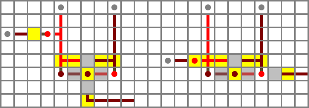
I initially placed the two filters directly opposite each other, but I ended up staggering them by two blocks to be able to fit the four control bit inputs between them in a two-block space. The ZX and NX busses will run on bridges and connect to the north filter, while ZY and NY run in tunnels and connect to the south filter. ZY is provided by a torch immediately under the protruding wired block, while the others run on stairs. The buses and their controls are included in the schematic file but left out of the image for clarity.
Full schematic file (Control bits in order: ZX, NX, ZY, NY)
Operations
The input filters produce the values X' and Y'. The next step is to add these and AND them. We’ll select the appropriate value based on the F flag later.
The adder is vandrien’s 5 × 7 × 3 design with no modifications. (This is the niftiest part of the entire design – if I had to design my own adder the ALU would be twice as big and significantly slower. Thanks, vandrien!) The Y' line is rerouted slightly. The switch at the top is CI, and the dangling wire at the bottom is CO.

Performance: The worst-case latency of the adder is five ticks, but carries are generated, handled and propagated in two ticks. By the time the carry ripple reaches the high-order element, its half-add will be complete, so the carry latency is all that matters for overall time.
I originally had a separate NAND gate on top of the adder. While decomposing the design from this writeup, I noticed that the X' wire wasn’t connected, but it was working anyway. Turns out I was accidentally extracting an AND from the adder and then NANDing that with Y'. The revised design just uses the AND from the adder directly. The source is either of the two opposing torches on the input side of layer 2 of the adder.
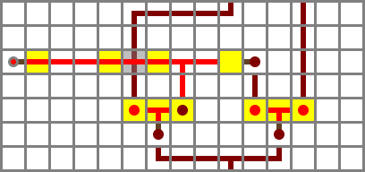
Output muxer
The next step is to select the appropriate preliminary output, O'. This requires a selector (muxer) circuit which takes three inputs, A, B and S, and outputs A if S is 1 and B if S is 0 – that is, (A ∧ S) ∨ (B ∧ ¬S). Here, S is in the middle to avoid crossing anything. (It will be routed through a tunnel.)
Performance: The latency of the muxer is three when changing S and two for anything else. In a full CPU, it’s reasonable to assume S (F) will be set before the other inputs are ready.
Plugged in:
Full schematic file (Control bits: ZX, NX, ZY, NY, F)
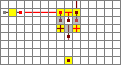
Output filter
The output filter is much like the input filter, but without a zero flag. It consists of an XNOR gate (wiki type C again) which takes O' from the muxer and ¬NO from a tunnelled bus.
Full schematic file (Control bits: ZX, NX, ZY, NY, F, NO)
And there you have it: a one-bit ALU. Here’s a block diagram:

The complete sixteen-bit version consists of sixteen of these side by side, with their carry flags chained together (low-order bit at the top, high-order bit at the bottom). I’ll spare you the details of working out the control bus wiring and stuff. The final design consists of eight identical two-element modules, with one set of bus repeaters per module, so the bus latency averages one tick per bit. Here it is, calculating its own redstone cost (2237 + 687 = 2924, or 1000 1011 1101 + 0010 1010 1111 = 1011 0110 1100):
Operations: It may not be immediately obvious how an ALU with only two operations is enough for useful computation, but the input and output flags let you do quite a lot. Some examples:
- Move = AND one input with all ones: ZY NY AND <source> <anything>
- NOT = move with negate: ZY NY NO AND <source> <anything>
- Clear (generate a zero): ZY ZX AND <anything> <anything>
- NAND: NO AND <a> <b>
- NOR = ¬X ∧ ¬Y: NX NY AND <a> <b>
- OR = ¬(¬X ∧ ¬Y): NX NY NO AND <a> <b>
- Subtract: NX NO ADD <a> <b>
For more, see slide 24 of this presentation.
Future directions
- The output muxer could probably be made smaller. It’s pretty much the first design that came to mind.
- It looks like I could shave off two columns of length, one on each side of the op logic block. The output muxer would need to be flipped over, and the control bit bus negated.
- The input filter section is seven wide (including insulation), while the other blocks are six. I think it’s possible to make the input filter section one block narrower by flipping the filters so the control inputs are on the outside, and sharing the inputs between adjacent elements. The input order would then alternate (the first element would have X₀ on top and Y₀ on the bottom, and the second would have Y₁ on top and X₁ on the bottom).
- Performance profiling. An add should take about 40 ticks, but I haven’t timed it.
- Carry look-ahead adder for moar faster. By which I mean “slightly less slow.”
- Other computer components: program counter, I/O controller, RAM, ROM. I probably won’t bother with all of them.
FAQ
- What’s the point?
I don’t understand the question.
Seriously, if you’re going to ask what the point is of doing something for fun in a game, why are you even on this forum?
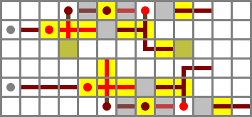
Improved input filter
30 October 2010 – 20:26
Improved input filter (and control bus) design, as outlined in first post.
The input filters now have the control inputs outwards, with one space between them, allowing the entire element to be one block narrower. The staggering is also removed, saving two blocks of length, with the control bus zig-zagging instead. Control inputs are torches (for isolation) on top of one torch in the appropriate bus repeater. The busses are negated.
This arrangement increases control bit latency. Wiring the low-order bit’s input differently could eliminate this delay for the add operation.
Since control bits are shared between adjacent input filters in different cells, the input bit order alternates: X₀, Y₀, Y₁, X₁, X₂, Y₂, Y₃, X₃. This will be rather inconvenient to use directly, but can be hidden by appropriate input bus wiring. The control bit order has also changed, to ZX, ZY, NX, NY.
The outputs adder stage will be moved up and back three steps, eliminating the staircase.
I’m not sure what I’m going to do about the output side yet.

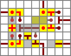
Improved output muxer
30 October 2010 – 20:11
Flipping the output muxer over and smashing it into the side of the adder worked out nicely, saving two columns. The select input (circled) is again fed by the NO bus repeater. The bus itself runs at ground level.
Schematic file (four bits wide)
The output negator XNOR can then be stuck right on the end of that, one step below, with no wiring gap. The control input is tunnelled, and connected to the circled block using two vertical torches. (The extra latency is not a problem, since the data has to go through all the previous blocks first.)
In-game prototype
31 October 2010 – 01:56
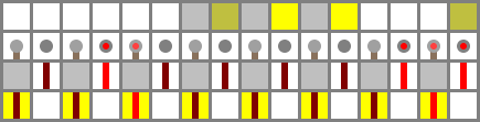
While waiting for the update server to come back to life, I built a one-bit element in-game.

Totally legit! Many sheep were seriously annoyed in the making of this device. (Wooden parts are control lines, wool is the structure of the logic element, stone is support structure, access ladders and so forth.)
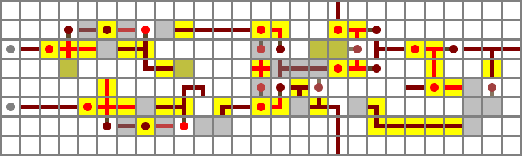
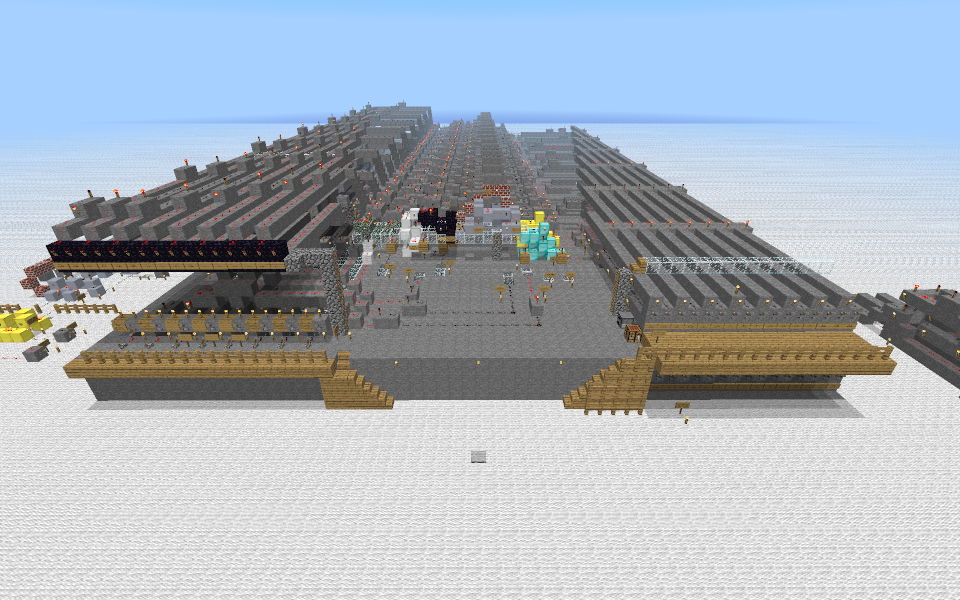
Here’s the full sixteen-bit schematic, again set to calculate its own component cost (including control interface): 1858 wires (0111 0100 0010) + 748 torches (0010 1110 1100) = 2606 redstone (1010 0010 1110). The 61 extra torches are the vertical-stack control line connections and input inverters, and the 379 fewer wires are space savings and simpler control busses.
The schematic is 26 × 104 × 12; 7 columns and 7 rows are interface, and 4 layers are control busses. The logic is 19 × (5 × 16 + 17 = 97) × 8.
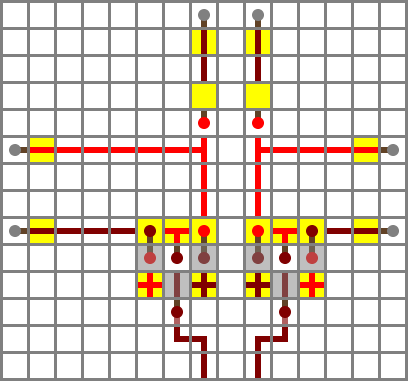
Load immediate and control & output busses
31 October 2010 – 04:42
In addition to the ALU instructions, the Hack architecture has only one more instruction, the @ instruction (or, more traditionally, “load immediate”). This loads a fifteen-bit value into register A. This can be integrated into the ALU by simply whacking another muxer on the end. This muxer takes the ALU output and the corresponding instruction bit (always zero for the high-order bit) as inputs, and the relevant control bit as the selector input.
Rather than add another switch to each element, I added a complete instruction bus. This can take either an @ instruction or an ALU instruction. Both use very simple encodings, so the decoder just has to run wires to the right control inputs. The instruction codings are as follows:
@ instruction:
0DDD DDDD DDDD DDDD
- ALU: Copy the instruction word to the output bus.
- Output controller: write ALU output to register A.
- Program counter: increment unconditionally.
Logic instruction:
111A CCCC CCDD DJJJ
The bits in each field are numbered from left (high-order) to right, so C₁ is adjacent to A and C₆ is adjacent to D₁.
- ALU: Set ZX to C₁, NX to C₂, ZY to C₃, NY to C₄, F to C₅, and NO to C₆.
- Input controller: if A is
0, set Y to register A. Otherwise, set Y to the contents of memory at the address specified by register A (referred to as RAM[A] or M). (X is always set to register D). - Output controller: if D₁, write to register A. If D₂, write to register D. If D₃, write to RAM[A] (presumably the value of A before updating it). Any combination is valid.
- Program counter: given condition bits NG (the high bit of the ALU output) and ZR (the NOR of all the output bits), jump to ROM[A] if (J₁ ∧ NG) ∨ (J₂ ∧ ZR) ∨ (J₃ ∧ (NG ⊽ ZR)), otherwise to the next instruction (dur). All combinations of J bits are valid.
(Note: RAM and ROM addresses are word addresses, or to put it differently, both the word size and the byte size is 16 bits.)
Here’s the instruction “DM=D+A” entered into the input bus (top right, levels 6–7):
The bits are in reverse order for routing reasons. (If you were standing in front of it facing south, it would be the right way around.) The three bits on the right are the logic instruction prefix (currently only the top bit matters, but the other two could be used for new instructions). The colour-coded ones are the control bits for logic ops; from right to left, ZX, NX, ZY, NY, F and NO. Destination bits D₂ and D₃ are set, but of course do nothing since there’s no output controller, and the condition bits are clear for no jump.
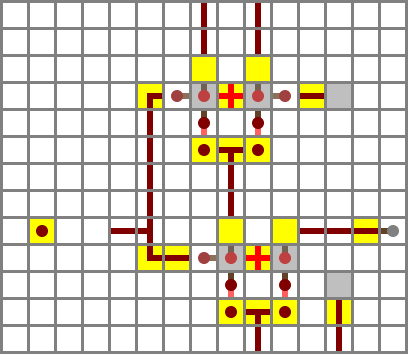
The logic element outputs are now in the middle of the schematic, so I added an output bus too (ending top right, layers 13-14). Here it is showing the value 5285 (0001 0100 1010 0101), once again backwards.

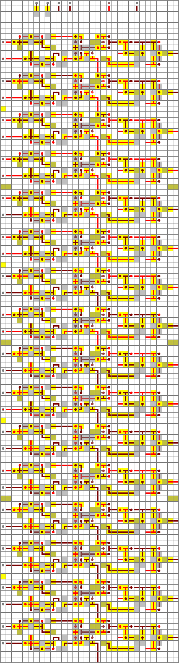
Schematic, set to calculate its own component cost in accordance with ancient tradition: 4232 wires (0001 0000 1000 1000) + 1053 torches (0000 0100 0001 1101) = 5285 redstone (0001 0100 1010 0101).
Design note: seven of the input bits are essentially duplicated in the control bit busses. This could be avoided, but the @ instruction would be slower, and it’s not clear that the recovered space could be used for anything since it’s underneath the output bus. I’ll revisit this if/when the other components are designed.
Input busses
31 October 2010 – 08:54
…and the logical next step is wiring the input busses. Nothing very interesting about them.
Schematic, set up to calculate 6357 (0001 1000 1101 0101) + 1177 (0000 0100 1001 1001) = 7534 (0001 1101 0110 1110).
ROM idea
7 November 2010 – 19:53
I haven’t done anything interesting (of relevance) this weekend, so here’s something boring instead: ROM. This will store the program, so the more you can fit in the available space the more the computer can do.
This is the cleverest ROM design I’ve been able to come up with, but it might not be the smartest – I suspect a less compressed design may end up taking less space when you consider stacking and control interfaces. I need to build several layers of each type, with output busses, to test this.
Each 1 bit is represented by a torch, and each zero bit (none in the schematic) by the absence of a torch. When the select line is off, the torches are powered and thus zero.
Half the bits feed into a bus above the module, and the other half a bus below the module. Feeding both into a compact bus above the module is possible, but requires more space and introduces delays.
I tried to come up with a way to avoid the parallel select line and space, but failed.
This module can be tiled in two dimensions without any space between copies. Repeater banks are required every three modules in the east/west direction. In the north/south direction, the two output busses are uninterrupted between words, so it’s easy to interpret the ROM as 8-bit or 32-bit elements just by putting a different output bus muxer on the end.
Here’s an eight-word matrix with output bus:

The rows are selected by putting a torch under a negated section of each row bus to force it to zero when not selected. The rows are then fed into the (positive) bus using the same technique. Note that there are currently two levers for each row, one for the low half-bus and one for the high, and these levers are negated while the column select levers are positive.
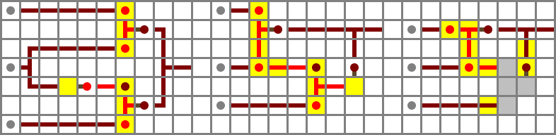
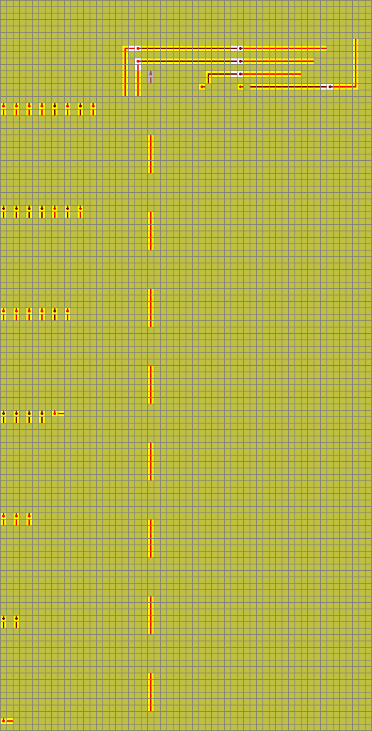
ALU download and exploded diagram
31 October 2010 – 21:31
I present, for your supremely geeky enjoyment, the ALU saved game.
(The ALU is not well lit. I strongly recommend setting the game to peaceful before loading.)
In the middle is the ALU, essentially per the schematic above. However, I’ve aded some lights, walkways and signs, and improved the interfaces (except the instruction input, because I got bored). The low-order ALU channel is colour-coded and signposted.
To the right in the picture is a prototype input interface with feedback lights. It’s too bulky to integrate easily, but lifting all the lines off the top of a minimum-width bus was fun.
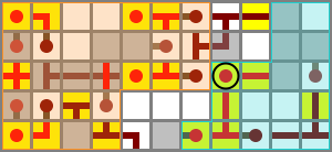
To the left is an “exploded” ALU channel. It implements the same logic as the ones in the full ALU, but is divided into distinct gates. The individual gates are mostly different from the ones in the real ALU, but they interact in the same way. It’s also colour-coded in the same way as the low-order “real” channel.
Section 1: input filters
The first section consists of the two input filters, the X input filter (right in diagram, diamond on map) and the Y input filter (gold). The main gate in each input filter is an XNOR gate (here wiki type A). The X input filter compares the NX control bit – lower right side input in diagram – with (NOT X OR ZX). If both NX and ZX are zero, the output on the X side will be X. If NX is set, it will be ¬X. If ZX is set, it will be 0, and if both ZX and NX are set, it will be 1.
For simplicity, I’ll refer to the filtered outputs as X and Y below, but this is misleading if any of the NX/NY/ZX/ZY control bits are set.
Logic:
X′ = (¬X ⋁ ZX) ↔ NX

Y′ = (¬Y ⋁ ZY) ↔ NY
Section 2: core functions
The second section is a full adder (made out of clay on the map). It consists of two almost identical modules, which are called half-adders. A half-adder takes two input bits, and produces a two-bit output ranging from 0 to 2. The possible combinations are:
| X | Y | out |
|---|---|---|
| 0 | 0 | 00 |
| 1 | 0 | 01 |
| 0 | 1 | 01 |
| 1 | 1 | 10 |
Note that the low bit of the output is equal to X XOR Y, and the high bit is X AND Y. The half-adder used here, which is identical to the second one in the “real” ALU, is similar to wiki XOR gate A, but rearranged so an internal NAND value can be pulled out (and inverted) on either side.
A half-adder is sufficient for a one-bit computer, but to add multiple bits we need to be able to take a carry input and add it to the sum. This is done with a second half-adder which takes the low bit of the first one as one input, and the incoming carry bit from the previous ALU channel as the other input. (This is called ripple-carry adding. There are faster approaches, but they take more space.)
The carry output is the OR of the two half-adders’ carry outputs. This value and the output of the second adder form a two-bit number which is the sum of the three inputs X, Y and CI:
| X | Y | CI | out |
|---|---|---|---|
| 0 | 0 | 0 | 00 |
| 1 | 0 | 0 | 01 |
| 0 | 1 | 0 | 01 |
| 1 | 1 | 0 | 10 |
| 0 | 0 | 1 | 01 |
| 1 | 0 | 1 | 10 |
| 0 | 1 | 1 | 10 |
| 1 | 1 | 1 | 11 |
The ALU has two core functions, ADD and AND. The AND (denoted A below) is acquired by a bridge (brick) from the second AND output of the first half-adder, along the right hand side of the diagram. The ADD value is denoted S, for “sum”.
Logic:
S = X′ ⊻ Y′ ⊻ Ci

CO = (X′ ⋀ Y′) ⋁ ((X′ ⊻ Y′) ⋀ CI)

A = X′ ⋀ Y′
Section 3: function muxer
The third section (obsidian) selects one of the two functions, based on the F control bit. If F is set, the ADD function is selected. Otherwise, the AND function is selected. In logic terms, that’s (F AND S) OR ((NOT F) AND A), here implemented as two basic ANDs, a NOT and a bridge.
Logic:
O′ = (F ⋀ S) ⋁ (¬F ⋀ A)
Section 4: output filter
The output filter (iron) inverts the output if the NO control bit is set. It’s a single XNOR gate like the ones in the input filter. Since the input isn’t inverted in this case, the NO bit is instead. This is equivalent to using an XOR gate, but is a bit more compact in redstone.
Logic:
O = O′ ↔ ¬NO = O′ ⊻ NO
Section 5: load immediate muxer
This isn’t included in the exploded channel. On the real ALU, it’s identical to the F mux, but one step down and made out of cossy mobblestone.
Using the full ALU
The instruction format is exactly the same as for theinternetftw’s CPU. However, mine doesn’t have any registers yet, so you’ll need to copy data from the output to the inputs. Since there’s no I/O, no clock is needed (beyond Minecraft’s update ticks); when the output bank stops changing, it’s finished calculating.
An optimization question
11 December 2010 – 16:27
CX gamer said:
Is it possible to apply pipelining to this, so the performance of multiple consecutive calculations can greatly be improved?
Probably not within the ALU itself. In a full CPU, you could use instruction prefetching (possibly with prediction of unconditional branches) and start issuing the next instruction slightly before the IO parts of the current one are processed, at least if there’s no memory read in the next instruction. Other obvious optimizations would be a one-word RAM cache, possibly with a second word of write buffer, and tight timing of the various dispatch stages. But in terms of actually being able to do anything, the main focus has to be keeping it small, so you can fit as much RAM as possible.
All high-level CPU optimizations, like pipelining, better algorithms and more powerful high-level instructions (like multiplication) are based on using more CPU die area to do stuff in smarter ways. Since Minecraft space isn’t subject to Moore’s law, we can’t really expect to see much of that sort of improvement in Minecraft computing, although if Notch adds SSI components (like one-block logic gates and latches) things could get interesting.
(Actually, there is one major space saving that can be done now: stacking the ALU and bus channels vertically. Avus, above, had the right idea, although the size of each channel eats up most of the optimization.)
I love this. This is amazing. I could NEVER do this. Thank you.
Could you possibly make something like an OLD Intel 8088 or 8085 processor? Not with stuff like RAM, just the processor itself?